
The Effects of Laser Pulse Width on the Ablation of Materials
By Osman A. Ghandour / Edited by Riad Ghandour

Comparison of the ns-ablation (left) and the fs-ablation (right) processes. In machining or surgery applications, the thermal effects in ns ablation can lead to a larger heat-affected zone, more collateral damage, and less precise machining compared to fs ablation. Inc.Ultrafast laser processing of materials: a review, Phillips et. al. , Vol. 7, No. 4 /December 2015 / Advances in Optics and Photonics. Figure used with permission from Clark-MXR
In this overview, we dive into the fascinating world of laser pulse durations—specifically, nanoseconds, picoseconds, and femtoseconds, how they affect the ablation of materials, and also a few real world examples of their applications to make understanding these seemingly complex topics much more digestible and intuitive.
When it comes to laser material processing, we generally work with two distinct pulse duration regimes. Long pulse durations, like those in the nanosecond range, can lead to a considerable heat-affected zone (HAZ) in materials. Why? Because their pulse duration often exceeds the thermalization time of most metals, which means that the heat generated can spread more widely than intended.
On the other hand, lasers operating in the femtosecond to picosecond range can significantly enhance the quality and precision of ablation compared to their nanosecond counterparts or even longer pulse durations. These pulse duration ranges provide outstanding results, especially for high-precision applications in micro- and nano-machining. For the most precise of material processing tasks, laser pulse durations of 10 picoseconds or less are ideal, and research suggests that the sweet spot for micro-machining metals like copper and stainless steel lies within the 10 to 100 picosecond range.
A couple of key metrics that help define pulsed lasers include pulse duration (or width) and pulse repetition rate (PRR)—the latter being an indicator of how many pulses are emitted each second. Additionally, both peak power (calculated from the energy of each pulse divided by the pulse duration) and average power (the pulse energy multiplied by PRR) are crucial for evaluating laser performance.
Now, when we hit the topic of pulsed laser ablation, it becomes clear that femtosecond and picosecond lasers shine (pun intended) when it comes to producing high-quality, precise processing. How is this achieved? These ultra-short pulses mainly interact with the electrons of the material rather than disturbing the entire lattice structure. This mechanism limits heat conduction significantly, which minimizes thermal and mechanical damage to the ablated area. Conversely, longer pulse durations, like nanoseconds, can lead to continuous heating and excessive heat conduction, resulting in uncontrollable melt layers that complicate the machining process.
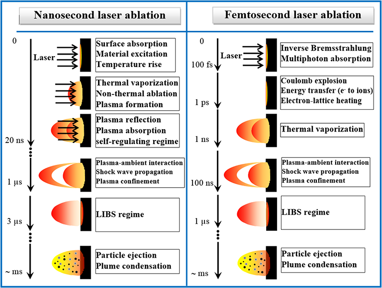
Approximate timescale comparison of pulsed laser energy absorption and ablation, along with the various processes, for nanosecond laser (10 ns) and femtosecond laser (50 fs) ablation in an ambient gas. Figure sourced from High Energy and Short Pulse Lasers, Chapter on Effects of Different Laser Pulse Regimes (Nanosecond, Picosecond and Femtosecond) on the Ablation of Materials for Production of Nanoparticles in Liquid Solution, Written By Abubaker Hassan Hamad, 07 September 2016
The ablation process begins with photon absorption, which triggers heating and photoionization in the targeted area. The state of the ablated material can differ quite a bit, depending on the amount of energy absorbed by the target. In low-intensity, short-pulse interactions, the absorption takes place primarily in the free electrons, and this leads to heat transfer to the lattice, a process often described through various dynamic models.
Pulse width also plays a vital role in determining ablation thresholds and penetration depths. Generally, longer pulse durations increases the threshold fluence while decreasing the effective energy penetration depth. As a result, interactions with nanosecond lasers can produce significant melt layers, creating a lot of headache for precision machining.
In the realm of picosecond laser ablation, these short pulses create a transient non-equilibrium state where electron temperatures are higher than those of the lattice. This condition often allows for material removal primarily through vaporization—without ever hitting the melting stage. Femtosecond laser ablation, on the other hand, occurs at such a fast pace that heat conduction can essentially be ignored. This translates into high kinetic energy, direct vaporization, and notably fewer thermal effects compared to nanosecond lasers. Femtosecond lasers also harness high peak intensities to kick off non-linear absorption processes. This includes phenomena like multi-photon ionization, where an electron absorbs multiple photons, and avalanche ionization, which enables a rapid increase in free electron density, causing a large-scale breakdown of target materials.

Nitinol stents micromachined with high precision using NKT Photonics’ femtosecond laser technology,
The first real world example of the importance of pulse width is when working with Nitinol, an alloy composed primarily of nickel and titanium known for its unique properties such as super-elasticity and shape memory. These characteristics make Nitinol particularly valuable in the medical field, especially for devices like stents and guidewires. In this case, utilizing a femtosecond laser as opposed to a nano- or picosecond is optimal since it provides the least HAZ—no melting, no burrs. Cut geometry and overall quality in, say for example a nitinol stent, is extremely important in medical device performance applications. Also you can probably imagine if you change the Nitinol metallurgy to something brittle because of the laser thermal effects, then you would run the risk of that stent being compromised within the human body (not good).
Another compelling example of the benefits of using femtosecond lasers can be seen in the drilling of gas direct injector (GDI) holes, critical components in combustion engines, responsible for delivering fuel into the combustion chamber with precision whilst under high pressure and temperatures. If these holes exhibit heat-affected zones (HAZ), we once again run the risk of altering the metallurgy of the stainless steel and can lead to a brittle structure at the edges. The brittle material poses a significant risk: under the extreme heat and pressure within the engine, fragments from this weakened material could break off and enter the combustion chamber, potentially causing catastrophic engine failures. By employing femtosecond lasers for this process, we can minimize or eliminate HAZ, preserving the integrity of the injector holes and significantly reducing the risk of such failures.
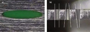
An elliptical hole (a) and tapered holes (b) drilled with the femtosecond laser-based R drill demonstrate enhanced geometrical flexibility, Laser Focus World, Nov. 13, 2013, Lasers & Sources, PHOTONICS APPLIED: INDUSTRIAL LASERS: The hole story: Femtosecond manufacturing improves automobile fuel efficiency, Michael Mielke
The last example is synthesizing black silicon. This involves adding high levels of dopants, like sulfur, to silicon beyond what is usually possible. By using femtosecond lasers to treat the silicon, one we can achieve higher concentrations of these dopants without forming unwanted byproducts. The process works by firing a series of rapid laser pulses at the silicon while adding different dopants. The result is black silicon, which has a special textured surface that reduces reflection and traps light more effectively. This enables it to absorb nearly all light from ultraviolet to near-infrared wavelengths, opening up exciting new possibilities for industrial applications.
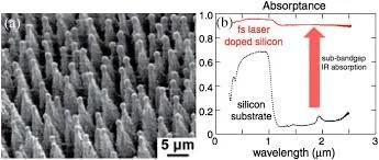
(a) Spiky, high-aspect-ratio, laser-induced periodic structures in silicon upon exposure to SF6 and fs-laser irradiation. (b) Absorption enhancement due to black silicon light-trapping conical tips and hyperdoping. Hyperdoping leads to strong sub-bandgap absorption, and texturing leads to increased absorption across the spectrum. Ultrafast laser processing of materials: a review, Phillips et. al. , Vol. 7, No. 4 / December 2015 / Advances in Optics and Photonics
I hope that by now, I’ve clearly established a few of the key differences between femtosecond, picosecond, and nanosecond lasers, and how those differences can significantly impact material processing, particularly in the realms of micro- and nano-machining. Femtosecond and picosecond lasers stand out for their precision and reduced thermal effects, making them the go-to choice for high-quality ablation tasks. In my next article, we will revisit this topic, but building on these insights, I’d like to share how these principles come to life in ablative scribing of solar cell structures, covered in a 2011 patent of mine.