
Laser-based Scribing of CIGS Solar Cell Material Structures for Monolithic Module Integration
By Osman A. Ghandour, edited by Riad Ghandour
Introduction
Seven years into my exciting journey of providing laser source, system, and process consulting and contract services to my valued customers, I have decided to start telling some compelling and interesting stories from my career in laser materials processing applications. One of those stories happened about fifteen years ago. This story still carries great relevance today in choosing a laser technology that provides an optimal innovative laser solution for certain material processing applications. Namely, it was about CIGS (Copper Indium Gallium Selenide) solar structure scribing for monolithic module integration.
At the time, I had no previous experience in solar cell and module technologies but I was brought on board because of the depth and breadth of my experience in laser materials processing technologies including those related to laser source, laser system, and laser process. I was asked to lead a team of solar engineers to find the optimal laser-based technology for performing the scribes known in the solar field as P1, P2, P3 scribes, the scribes necessary for monolithic CIGS solar module integration.
Discussions
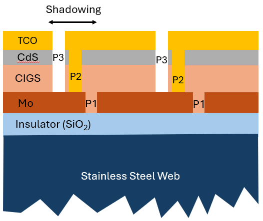
Figure 1. A schematic illustration of a cross-sectional view of a portion of a monolithically integrated module, including interconnected cells [1].
The CIGS solar material was manufactured on the basis of roll-to-roll stainless steel web. Once a laser scribing process was determined, the solar cell structure of coating and laser scribing would have been represented as shown schematically in figure 1 [1]. A stainless steel web would be coated with an electrical insulator layer such as SiO_2 on one side. Then a molybdenum based back contact layer would be coated on the insulator layer. P1 scribe would be formed on the molybdenum layer stopping at the insulator layer. After that, CIGS layer would be deposited on the molybdenum layer. Then, a buffer layer, made of CdS (cadmium sulfide) for example, would be deposited on the CIGS layer. P2 scribe would be formed in the buffer and CIGS layer stopping on the molybdenum layer. Subsequently, a TCO (thin conducting oxide) layer would be deposited on the buffer layer. P3 would then be formed on the TCO/buffer/CIGS layer stack stopping on the molybdenum layer. With that the solar cells would be interconnected in series and a web section with a certain length containing a number of cells would form an array of cells to be used in the monolithically integrated CIGS solar module.
What makes P1, P2, and P3 scribes optimal:
The scribes have to be as minimum in width as possible. This is because, as shown in figure 1, the total width of P1, P2, and P3 is a shadowed area of the solar cell structure that has no current generation capability reducing the module efficiency.
The scribes have to be melt free. Melting on the edges of the scribe can weld the solar materials layers together causing shunting that reduces efficiency
The scribes have to be particle free. Producing particles during scribes can interfere with the next coating steps causing efficiency reducing shunts
The front contact TCO layer would be 100 to 1000 nm thick [1]. The semiconductor CIGS/buffer layer would be 500 to 3000 nm thick [1]. The molybdenum-based back contact layer would be 100 to 1000 nm thick [1].
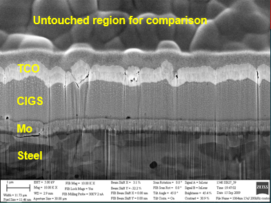
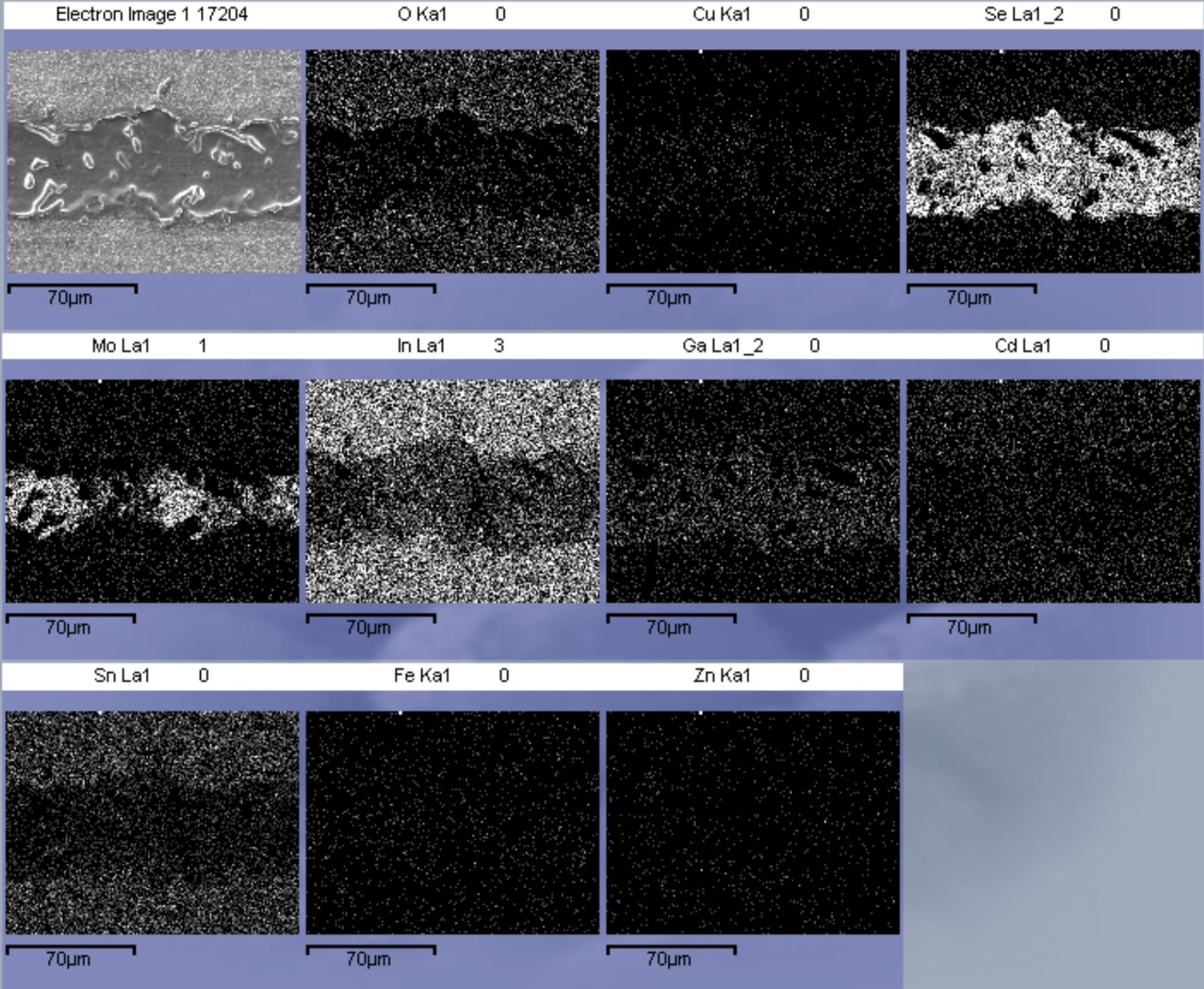
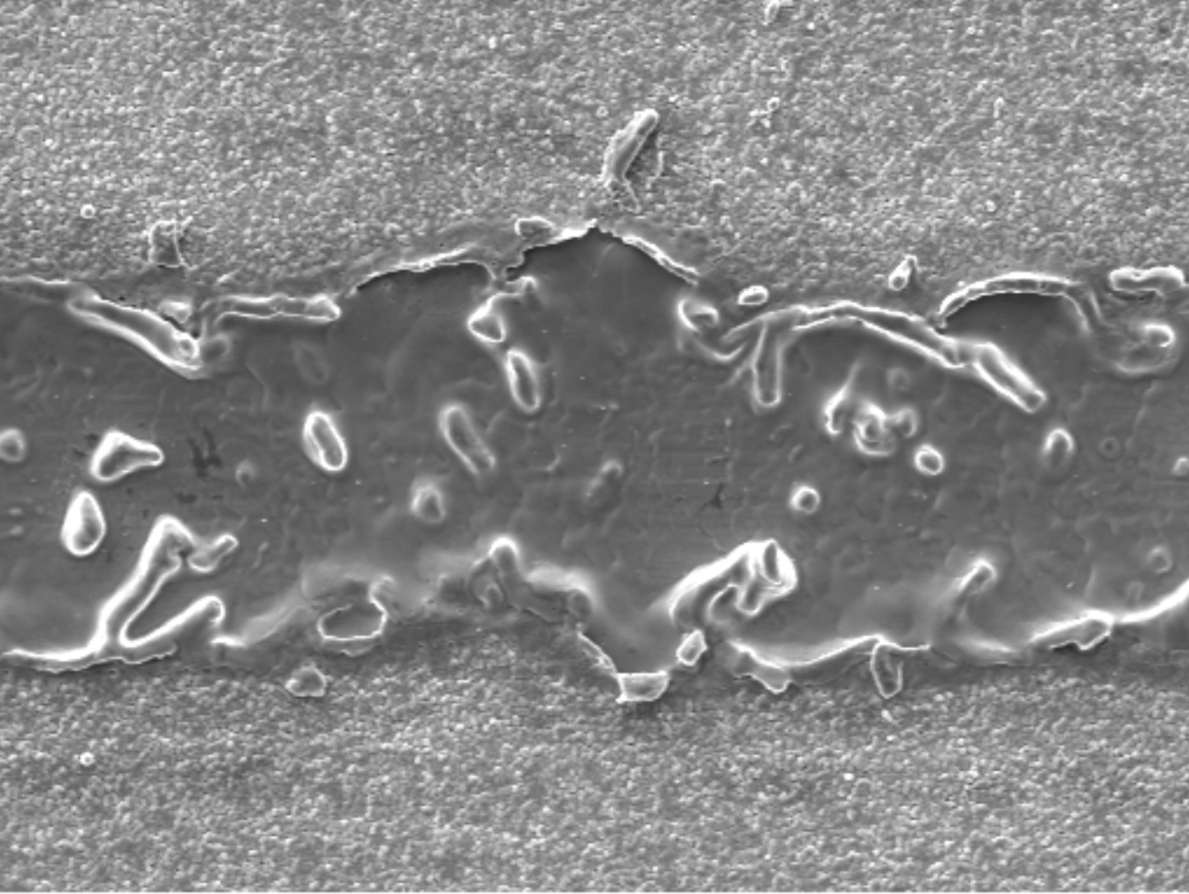
Figure 2. FIB SEM cross-sectional view of the untouched stainless-steel-based CIGS solar cell sample sent to the outside laser apps labs [1]. Front contact TCO layer: 690 nm. CIGS/buffer layer: 1600 nm. Back contact molybdenum layer: 540 nm
As the laser SME (subject matter expert) on the team, I led the effort to obtain solar structure samples — sections of the solar structure web — and send them to outside companies providing laser source and laser system products. The applications teams at these outside companies received instructions from me and my team on developing and optimizing the laser scribes and then went ahead and ran the process development and optimization. The laser source technologies utilized in this effort were nanosecond, picosecond, and femtosecond lasers. We specifically asked for an optimal P3 scribe with a detailed report on the process development and optimization.
When we received the samples back, we asked our analytical lab team to perform top-view SEM (Scanning Electron Microscope) microscopy, cross-sectional FIB (Focused Ion Beam) SEM microscopy, and EDS (Energy Dispersive Spectroscopy) elemental mapping to measure and examine the scribes. Figure 2 shows a cross-sectional FIB SEM of a typical untouched solar sample similar to the samples we sent out [1]. In this sample, the front contact TCO layer was about 690 nm thick [1], the CIGS/buffer layer was about 1600 nm thick [1], and the molybdenum-based back contact layer was about 540 nm thick [1].
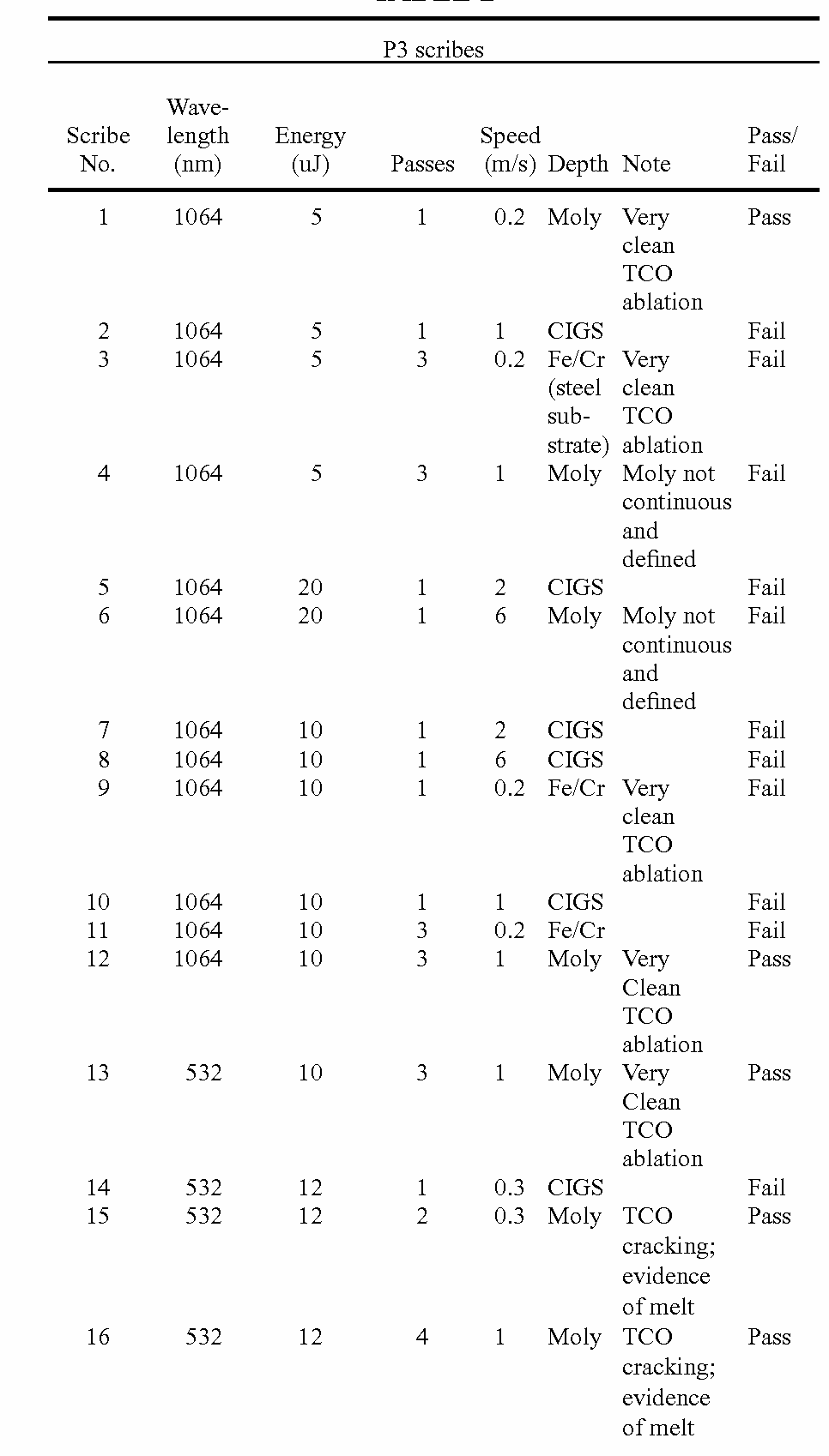
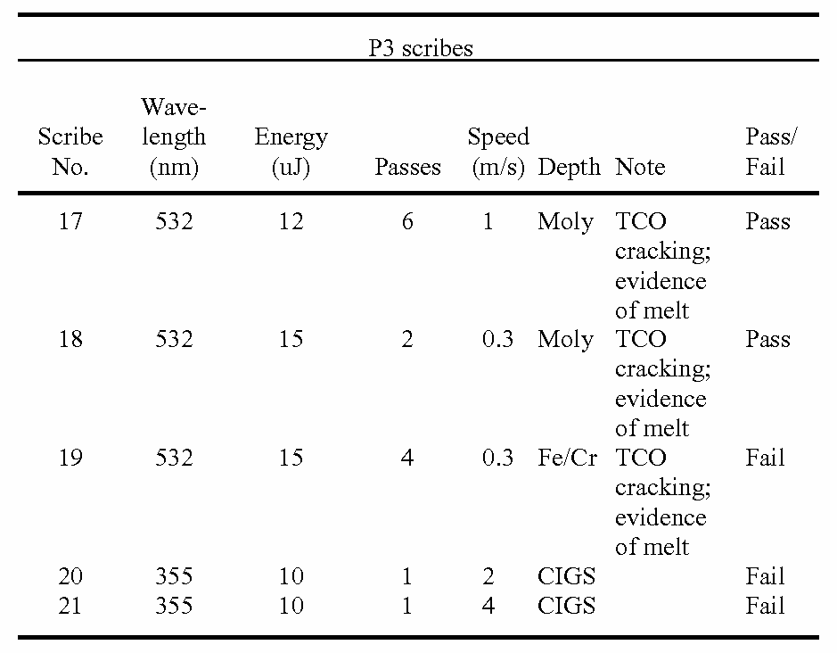
Table 1. Data on P3 scribes [1]
P3 scribes on SST/Mo/CIGS/buffer/TCO solar structure samples were performed at the outside laser apps labs using 355 nm, 532 nm, and 1064 nm wavelength lasers with pulse-width durations in ranges including nanosecond, picosecond, and femtosecond range. The total thickness of the CIGS/buffer/TCO layers, the material to be removed in P3 scribe was about 2830 nm [1], with the CIGS layer thickness being about 1600 nm [1]. For each laser wavelength and pulse width, laser fluence, energy level, scan speed, and passes were optimized based on scribe width, consistency, depth, and cleanliness. Depth and cleanliness of the scribes were assessed using EDS elemental mapping. The scribes were also closely examined for evidence of melting by top view SEM and cross-sectional view FIB/SEM. Based on these criteria the data for the various scribes were organized in table 1 [1]. The data showed the conditions of each scribe and the final result of whether or not the scribe had passed.
Laser scribes able to successfully scribe down to the molybdenum layer were deemed to have passed. Only 1064 nm (scribe nos. 1 and 12) and 532 nm (scribe nos. 13, 15, 16, 17 and 18) lasers successfully scribed down to the molybdenum layer [1]. Of these, only the 1064 nm scribe lines displayed no evidence of melting [1]. Evidence of melting was most pronounced for 355 nm, followed by the 532 nm [1]. The scribe at 1064 nm produced very clean lines in the TCO layer, showing no evidence of melting [1]. P3 scribes were also performed using a 1064 nm nanosecond laser. Cracks and melting residues were observed on these scribes [1].
Figure 3 shows EDS elemental maps and SEM top views of a P3 scribe whose process was developed and optimized based on 355 nm nanosecond laser [1]. The scribe had excessive melting associated with it. The width of the scribe was about 50 µm. Minimal complete scribe width is important in order to minimize shadowing of the 3 scribes P1,P2, and P3 that would negatively impact efficiency. The molybdenum signal is strong indicating that the scribe went down to the molybdenum layer. But, because of the melt splatter the molybdenum signal within the scribe was not consistent. Such a scribe was considered a failure.
Figure 4 shows EDS elemental map as well as SEM top view and SEM cross-sectional view of a P3 scribe whose process was developed and optimized based on 1064 nm picosecond laser [1]. The scribe was virtually free of melting. The width of the scribe was about 45 µm. The molybdenum signal was strong indicating that the scribe depth was all the way down to the molybdenum layer. The cross-sectional view SEM showed that the scribe had fractures on the edges indicating that the scribe was mechanical in mechanism. The speed for this scribe up to 4 m/sec
(a)
Figure 3. 355 nm nanosecond laser P3 scribe [1]. Width: ~50 µm. Notice the strong melt splatter on the scribe edges and within the scribe. (a) Top-view SEM with EDS elemental map. (b) Top-view SEM.
(b)

(a)
Figure 5 shows EDS elemental map as well as SEM top view and SEM cross-sectional view of a scribe whose process was developed and optimized based on 1030 nm femtosecond laser [1]. The width of the scribe was ~ 34 µm. The scribe was complete with a strong and consistent Molybdenum signal. The cross-sectional view SEM photo showed slight melting along the scribe edge in a transition region that was <1 µm in width. This scribe speed was less than 1 mm/sec making it economically nonviable. The slow speed and melting indicated that this femtosecond scribe was a failure. The data for this scribe was not included in table 1.

(b)
Figure 4. 1064 nm picosecond laser P3 scribe [1]. The width of the scribe was about 45 µm. Notice TCO fracture on the edge of the scribe indicating that the scribe mechanism was mechanical. a) Top view SEM with EDS elemental map b) Cross sectional SEM view.
The femtosecond laser scribe would have had the minimum heat affected zone (HAZ). But, it still showed some melting. This is because for the femtosecond laser at a typical spot size that’s comparable to that of the picosecond laser the peak intensity of the laser is high enough to induce nonlinear absorption rendering the removal process mechanism direct vaporization on most of the scribe with a tiny <1 µm melt dominated transition region on the edges. The picosecond laser would have a bigger HAZ and would have produced some melting but the scribing process material removal was mechanical in nature removing the material over the scribe and slightly outside of it.
As shown in figure 4 the 1064 nm laser provided melt and particle free scribing that had passed the scribe quality criteria [1]. In conventional laser scribe processes, film is removed by a mechanism that includes melting: laser pulse energy is absorbed, leading to temperature increase, which in turn leads to thermal expansion and melting. Laser energy on the molten material in turn causes splatter, which when solidifies results in particles welded to other layers [1]. The solidified melt pools and particles can be a major cause of shunt formation between front and back contacts in a cell, which is detrimental to device performance [1]. This is the case with nanosecond laser. Also, based on the study herein the femtosecond laser because of its extremely high peak intensity its energy is absorbed in the material layers via nonlinear absorption which would drive direct vaporization material removal over most of the scribe with slight melting observed over a tiny transition region of 1 µm in width

(a)

(b)
Figure 5. 1030 nm femtosecond laser P3 scribe [1]. The width of the scribe was about 34 µm. Notice slight CIGS melting on the edge of the scribe indicating that the scribe mechanism was direct vaporization with some slight melt on the edge in a transistion region that is <1 µm in width. a) Top view SEM with EDS elemental map. b) Cross sectional SEM view.
The 1064 nm picosecond laser successfully scribes the solar structure with virtually no melting or particle formation [1]. Using ultra short picosecond pulse laser beams of certain wavelengths and pulse widths, P1, P2 and P3 scribes in CIGS solar structures were produced without melting or particles associated with typical scribing processes [1]. Specifically, it was found that with a 12-15 picosecond pulse width and 1064 nm wavelength the laser optical penetration depth is on the order of or greater than overlying film thickness. Once the laser beam passes through the overlying layer and is absorbed by the layer beneath, a strong ablation shockwave is produced in the underlying layer resulting in mechanical shock removal of the overlying layer with virtually no melting or particles as shown in figure 4. P1 scribing of molybdenum coatings on a flexible SiO_2 layer coated on stainless steel web using 1064 nm and a picosecond range pulse width would also produce scribe lines with virtually no melting or particles. This was determined based on using this type of laser in scribing molybdenum layers similar to the ones used in the CIGS solar structure described here on glass plates [1].
It is believed that the improved scribing is due to producing the scribes via a shockwave produced at the interface of the layer to be removed and the underlying layer. This mechanism is possible only by selecting the right wavelength which produces an optical penetration depth on the order or greater than the thickness of the layer to be removed and by selecting an optimal laser peak intensity. Such mechanism is dominated by mechanical removal without melting (like the case with nanosecond laser) or direct vaporization with slight melting (like the case with femtosecond laser).
To produce an ablative shockwave that removes a top layer without melting, the following conditions must be met [1]:
1) The laser beam has a wavelength that provides an optical penetration depth on the order of, or greater than the thickness of the top layer,
2) The absorption coefficient of the underlying layer at that wavelength is greater than a threshold minimum necessary for the underlying layer to absorb the energy and allow a high enough absorbed peak intensity to produce the shockwave,
3) The pulse width is small enough to provide the requisite peak intensity to produce the shockwave, but not so small that it results in non-linear absorption in the top overlying layer.
Optical penetration depths for various example solar cell layers and laser beam wavelengths are provided below in Table 2 [1]. The optical penetration depth is calculated as follows:
Optical penetration depth = 1/α = λ / (4·π·k) [1]
where α is the absorption coefficient, λ is the wavelength, and k is the extinction coefficient for the material at that wavelength.
Table 2 presents examples of optical penetration depths for wavelengths in typical solar cell layers [1]. Determining laser beam wavelength that can produce an ablative shockwave as describe above may be done with reference to Table 2 or by determining an optical penetration depth for a particular material and wavelength. For example, to remove a CIGS layer of 1000 nm, Table 2 shows that wavelengths of 1000 nm or 1040 nm may be used [1] (both having optical penetration depths greater than 1000 nm).
Multiple layers may be scribed simultaneously, if they are transparent at the laser beam wavelength and the optical penetration depth exceeds that stack thickness [1]. For example, a TCO/buffer layer/absorber layer stack is P3 scribed with a 1064 nm, leaving an underlying back contact layer. For the purposes of this description a top layer or overlayer may include multiple layers that are optically transparent at a particular wavelength. Optical transparency may be characterized by the extinction coefficient, k, which characterizes absorption of electromagnetic energy of a wave propagating through a material [1]. As indicated above, optical penetration depth is 1/α = λ/(4.π.k). Transparent materials are characterized by k close to zero, and a corresponding high optical penetration depth.
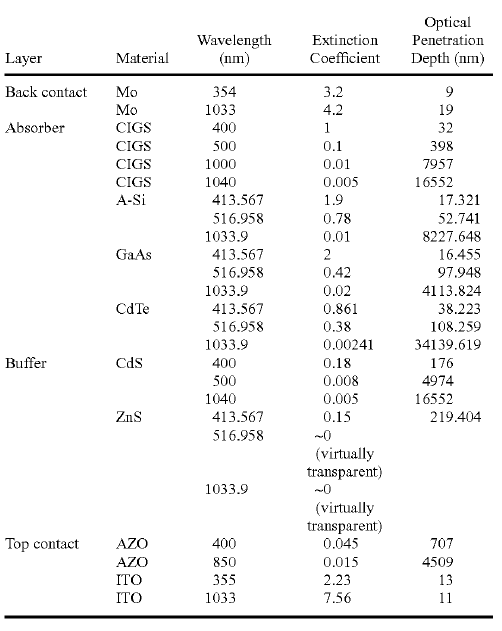
Table 2. Optical penetration depths of various solar cell layers [1]
While an optical penetration depth large enough to act on the underlying layer is a prerequisite for the ablative shockwave removal mechanism illustrated in figure 4, the peak intensity of the laser pulse must also be appropriately chosen to produce the ablative shockwave [1]. Peak intensity of the laser pulse is inversely correlated to the pulse width:
Peak intensity = Peak Power / Spot area
Peak power = Energy / (full-width half-max pulse width)
This represents one way to define peak power. Base-to-base pulse-width or 90% pulse-width, and other pulse width representations are examples of other ways to refer to pulse width that can be used in the formula for peak power [1]
Above a threshold pulse-width for a particular laser energy and spot size, the peak intensity is not high enough to generate a strong ablation shockwave. Scribing a CIGS/buffer/TCO layer having a thickness on the order of 1000 nm with a wavelength of 1064 nm was attempted using pulse widths of nanoseconds (10-9) and picoseconds (10-12). Descriptions of pulse widths in these units include tens of each units, e.g. tens of picoseconds. It was found that even with a wavelength of 1064 nm (and thus the requisite optical penetration depth) melt-free scribing was obtained only with pulse widths in the picosecond range. In the nanosecond pulse width range the peak intensity is not high enough to produce a strong ablation shockwave. If the pulse width is decreased too much down to the femtosecond range nonlinear absorption in the overlying layer to be removed kicks in. Hence, the optical penetration depth does not extend beyond the layer to be removed in order to produce the mechanical removal mechanism discussed herein.
Summary
Although this story happened about 15 years ago, the candidate laser sources evaluated at that time remain highly relevant in today’s laser industry.
One of the most important requirements for the P1, P2, and P3 scribes used for monolithic CIGS solar module integration is lack of melting. Nanosecond laser failed as a source for this application due to excessive melting. From there, one might intuitively expect that femtosecond lasers - known for their minimal heat affected zone (HAZ) - would be the ideal choice. However, it is important not to make assumptions when it comes to laser applications. Instead, each application must be thoroughly investigated through systematic experimentation including, when necessary, collaboration with external laser application labs.
In this particular case, the best quality scribe that’s completely free of melting and particles while maintaining reasonably narrow scribe width on the order of 45 µm was surprisingly achieved using a 1064 nm picosecond laser rather than the 1030 nm femtosecond laser. In addition, the 1064 nm picosecond laser also proved to be the most economically viable option supporting scan speeds up to several meters per second and possibly reaching as high as 4 meters per second.
According to this study, the optimal scribe quality was achieved through a laser-induced mechanical removal mechanism. At the 1064 nm wavelength the optical penetration depth was comparable to or bigger than the thickness of the layer to be removed. This allowed the laser energy to pass through the weakly absorbing or even transparent top layer and interact with the absorbing layer underneath. The laser peak intensity was sufficient to generate a strong ablation shockwave at the interface between the layers. This resulted in a “shock-off” effect – mechanically ejecting the top layer without significant thermal and mechanical damage. The resulting scribe was relatively narrow and free of melting and particles.
By contrast, the femtosecond laser operating with extremely short pulse durations produced peak intensities that were too high leading to nonlinear absorption in the top layer. The primary material removal mechanism became direct vaporization which, while effective, also introduced some melting. This melting was observed in a very narrow transition region at the scribe edges that was approximately 1 µm in width. As a result, the femtosecond laser scribes exhibited slight but measurable thermal effects.
Reference
[1] Ghandour et al., US Patent 8,048,706 B1, “Ablative Scribing of Solar Cell Structures”, November 1, 2011.